Engineers chart semiconductors on the scale of atoms
Spanning fewer than a thousand atoms, the electronic devices on semiconductor chips have become so miniscule they defy most efforts to characterize them. Now for the first time, engineers have demonstrated a way to image these vanishingly small devices by mapping them atom by atom.
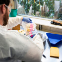
In a study published in the August 1 issue of Applied Physics Letters, John Booske, a UW–Madison professor of electrical and computer engineering; and Keith Thompson, David Larson and Tom Kelly of the Madison-based company Imago Scientific Instruments; used Imago’s local electrode atom probe (LEAP) microscope to pinpoint individual atoms of boron-a common additive, or dopant, in semiconductors-within a sea of silicon atoms.
The precise placement of dopants has long concerned engineers because these elements control the electrical properties of silicon transistors-the tiny, voltage-controlled switches found by the millions on semiconductor chips. But as manufacturers have relentlessly reduced the size of transistors in order to squeeze more of them on chips, locating dopants has become progressively difficult.
“As we start studying and manufacturing electronic devices whose sizes are approximately 100 nanometers or less in all three dimensions, and we want to know where the dopants and the defects are, we’re getting into the realm of asking, ‘Just where are all the individual atoms and what type of atoms are they?'” says Booske.
With its ability to analyze roughly 50 million atoms an hour, LEAP can now routinely map the properties of even the tiniest semiconductor devices, producing findings that manufacturers can use to diagnose and correct the defects underlying electrical failures. Until now, a lack of suitable tools has forced industry to pursue a laborious and largely blind, trial and error approach to new device development, says Thompson, a former Texas Instruments employee who is now senior applications engineer at Imago.
LEAP is an advanced atom probe microscope invented by Kelly. A former UW–Madison professor of materials science and engineering, he left the university to start Imago with Larson, then a graduate student. To create images, Kelly’s instrument applies voltage to a specially prepared, needle-shaped sample, ripping atoms from the sample’s tip one by one. An electric field then pulls the charged atoms to a detector, which identifies them and records their location in the original specimen.
The paper’s results represent the first practical application of LEAP to semiconductors, says Thompson. Atom probing has traditionally been restricted to metallic specimens because of the need for them to readily conduct electricity.
The project originally began when Thompson was a postdoctoral researcher in Booske’s laboratory and the pair was studying silicon transistors. Both to achieve faster switching and fit more transistors onto a single silicon wafer, manufacturers have been decreasing the size of the “gate”-the part of the transistor that controls switching-by 30 percent every two years.
“As the gate gets smaller, every other feature in the device has to get smaller–you can’t just shrink one part,” says Thompson. “And as this happens, you really start worrying where every atom is.”
For atomic-scale transistors to function properly, boron must be implanted at very high concentrations within the first 200 to 300 atomic layers of the silicon surface, he explains. But a critical heating step for making transistors often causes boron atoms to diffuse more deeply, ending up in regions where another dopant, usually arsenic, resides.
“Before, when semiconductors had feature sizes of one to two microns (1000 to 2000 nanometers), a 20- to 30-nanometer region of overlap between the dopants resulted in an error of only two percent,” says Thompson. “Now, with feature sizes of 30 and 40 nanometers, even 10 nanometers of inter-diffusion represents a 25 to 30 percent error.”
Booske and Thompson devised a microwave rapid-heating technique that they believed would limit diffusion. But the pair soon realized the system’s minute scale left them no way to confirm the boron atoms were staying put.
“After searching around, we came to the conclusion that the only technology with the potential to make these kinds of measurements would be Imago’s LEAP instrument,” says Booske. “So, Imago provided the instrument facility and Keith and I worked on the materials and specimen preparation end of things.” Eventually, the collaboration proved so successful Imago hired Thompson as a full-time employee.
LEAP has now revealed in precise, three-dimensional detail that rapid-heating techniques do indeed cause boron to spread from its original location. For example, images of boron-laden regions atop the transistor gates show dopant atoms amassed like pebbles in the crevices between seemingly boulder-sized crystals of silicon.
Movement and clustering of boron “is something that had never been experimentally verified,” says Thompson. “It had only been assumed. Physics says that it should happen, but there was never a technique to actually show it happens.” In one boron pile-up at the junction of three silicon grains, the scientists counted exactly 264 atoms, a feat of enumeration not possible with any other method.
Because clustering can lead to electrical failure, the results demonstrate the need to further investigate rapid-heating techniques. With the new information LEAP provides, semiconductor manufacturers can now do just that as they continue their push to miniaturize chip components.
“The timing is right for an instrument like LEAP to come along,” says Booske. “The need is there.”
Tags: biosciences, business, research
-
UW–Madison’s reach throughout Wisconsin adds up to $38.9 billion a year
The university supports more than 287,000 jobs and helps drive private-sector growth.
-
‘Being part of something bigger than you’ with Badger Volunteers
UW–Madison students head into the local community to find purpose and make a difference.
-
UW–Madison again named a ‘new Ivy’ by Forbes
The university was selected as one of the best in the country at "preparing and graduating the talent" that meets today's workforce needs.
-
UW–Madison graduate programs ranked among the nation’s best by U.S. News
Nearly 20 programs ranked in their respective Top 10 lists, shining a light on the breadth and depth of the university’s graduate offerings.